CMOS 101 - Understanding integrated circuits of the CMOS family
October 4, 2019 • tutorial
Microcontrollers are great, but sometimes it doesn't hurt to think outside the box a little bit. In this tutorial we will go through the basics of integrated circuits (ICs) of the CMOS family, including counters, logic gates, encoders & decoders, shift registers, flip flops, and others. Knowing when you can use a CMOS IC to solve a simple problem can and will make your life easier!
In this tutorial we will go through the basics of CMOS ICs. How do you power them, what should you keep in mind, and, most importantly: how can they make your life simpler?
CMOS: what it is, and why it is better than TTL
First off, CMOS stands for complementary metal-oxide-semiconductor. Great, now what? CMOS does not stand for one special integrated circuit or device but it stands for the technology that is used to build it. If you zoom in, any integrated circuit (or IC for short) is made of dozens, hundreds, or thousands of little transistors that are etched into a silicon wafer:
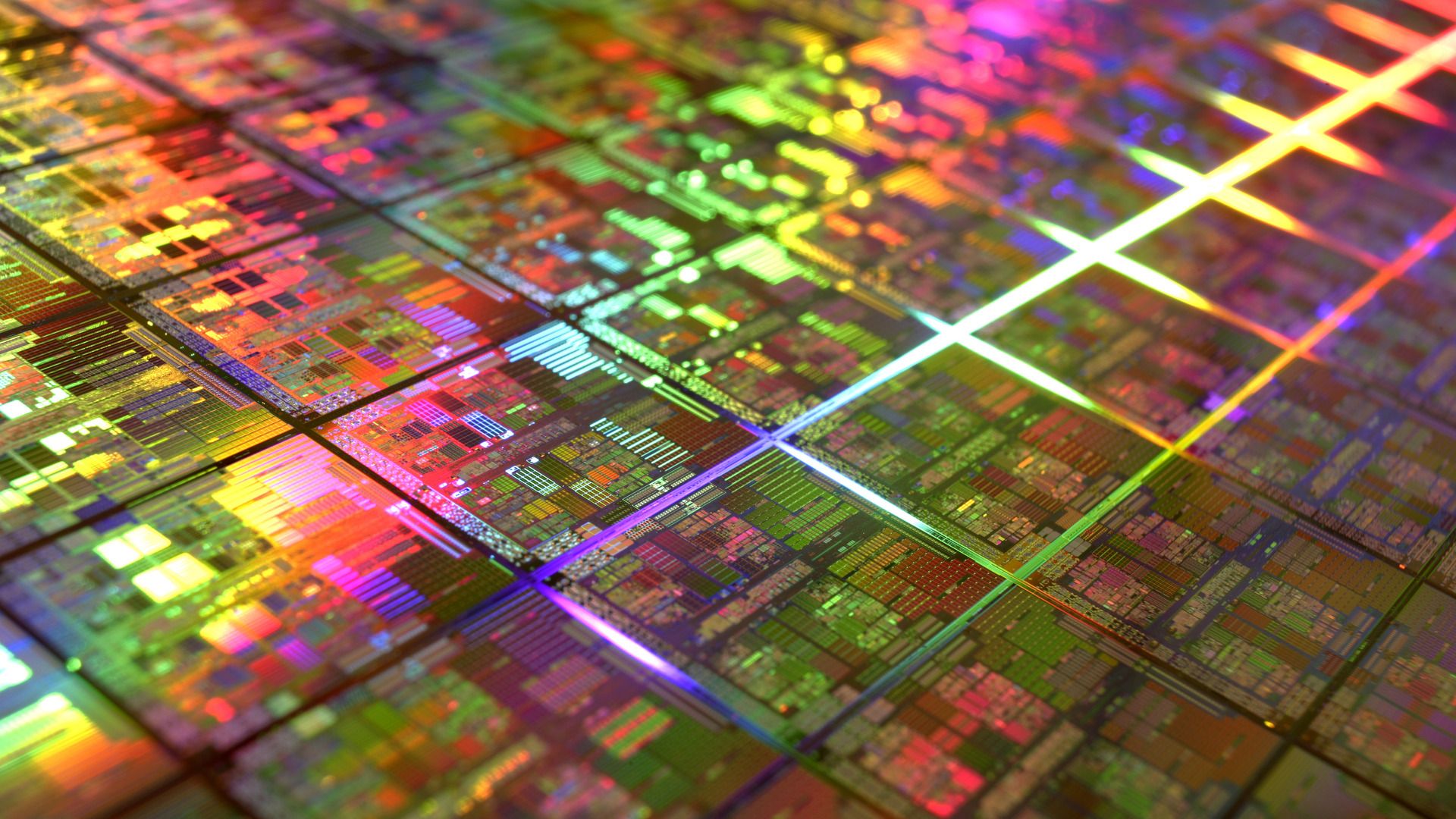
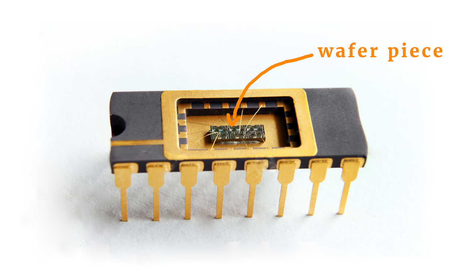
And yes, these wafers actually shine like rainbows, much like a CD! Why is that? The tiny structures etched into the crystalline silicon refract the optical wavelengths differently, depending on the angle, thereby creating a rainbow pattern. With CDs it is very similar: the tiny rows of data are a substructure that also refract the light :) Here you can see the inside of an integrated circuit:
OK, but what does that have to do with CMOS? CMOS makes use of so-called metal-oxide field effect transistors (or MOSFETs) for short. Those transistors are typically used in pairs, which is what the word complementary stands for. To understand the significance it is worthwhile to talk about TTL as well. TTL stands for Transistor Transistor Logic and represents another method of building logic circuits, this time using regular bipolar junction transistors (NPN and PNP types). This method was very popular in the 1970s, but was eventually superseded by the more efficient CMOS technology.
Here you can see a simple inverter in CMOS (left) and TTL (right). They each take an input, call it A, and transform it to its logical opposite, call it A. Here you can see the schematic:
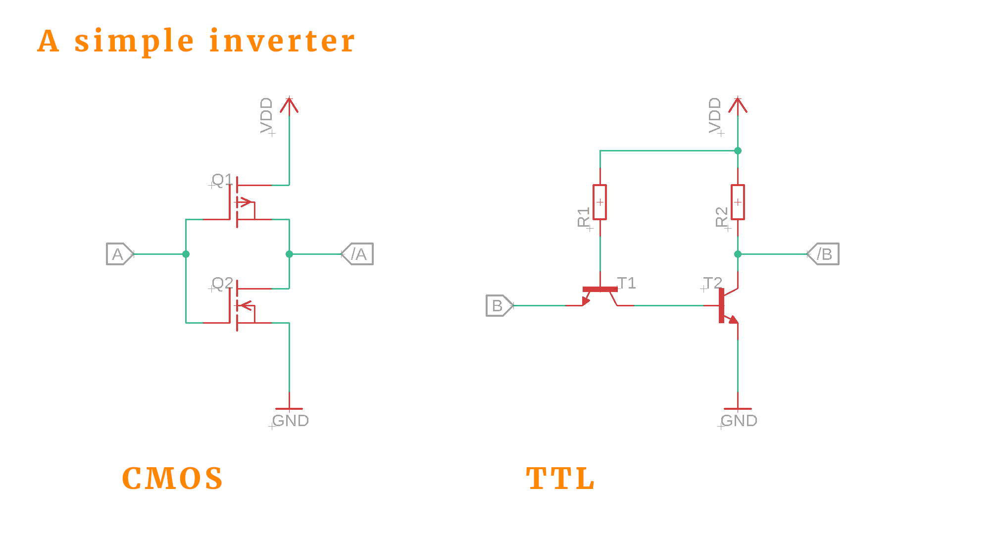
The disadvantage of the TTL circuit is that it consumes power in both states: both when its input B is 1 (high) or 0 (low). That is because the NPN transistors T1 and T2 need a small current to flow from the base to the emitter to become conducting. It is a small current, nothing excessive, but it is non-zero. Now imagine that you have not one or ten of these circuits, but hundreds or thousands. I think you can see why this technology has some problems if it is scaled up.
CMOS technology, on the other hand, works differently. It makes use of field effect transistors which need a voltage (not a current!) to become conducting. There is only a small current necessary whenever the state of the input changes from 1 to 0 or from 0 to 1. In the static case, when the input doesn't change, CMOS-type circuits consume far less power than their TTL counterparts. So it is really no surprise that CMOS eventually took over.
CMOS basics: power supply, filter capacitors, and sockets
The operating voltage for CMOS integrate circuits (ICs) is 3-18V. This is a huge difference to TTL ICs which only work with 5V. This wider operating voltage of CMOS ICs makes them ideal for battery-powered operation. In the context of this tutorial, the positive voltage supply is called VDD and the ground potential is called GND (as usual).
Most CMOS ICs come in a so-called DIP package, which stands for dual in-line package:
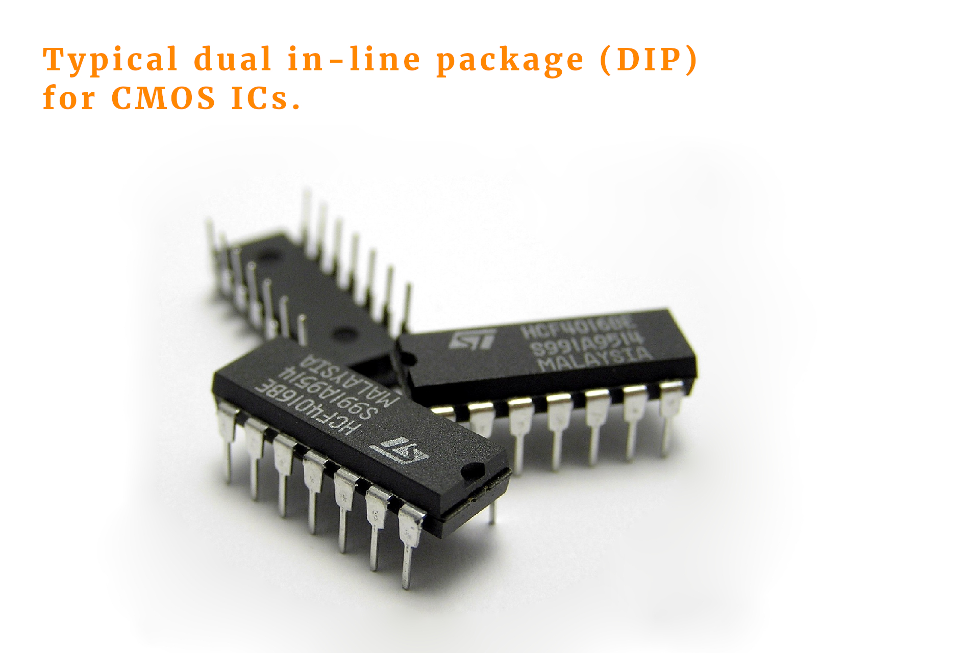
There are a few characteristic details about DIP that are important to know. Here you can see a DIP16 package:
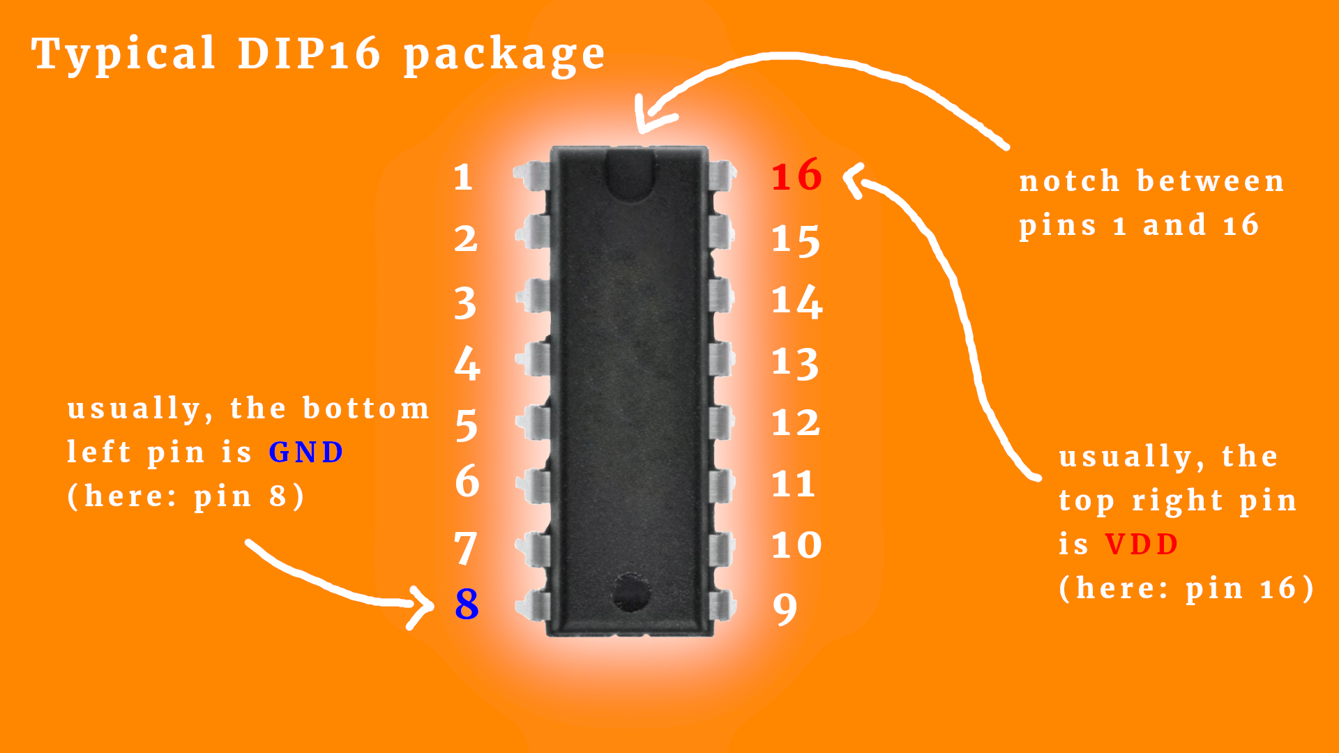
CMOS IC packages can be classified by the number of pins. A package with 16 pins is called DIP16, and so on. Pin 1 is the top left pin, and pin 16 is the top right. Between these two pins you can find a pronounced notch. Sometimes you also find a smaller mark between the bottom two pins, but this is just a leftover from the injection molding of the plastic housing and should not be confused with the notch. Generally, the GND pin is usually at the bottom left, and VDD is the top right.
When using breadboards you can just plug in CMOS ICs into the breadboard directly. When using a printed circuit board (PCB) it is sometimes helpful to work with a matching socket instead. If the IC breaks, for some reason, it will be easier to replace it. here you can see a selection of sockets for the DIP16 package:
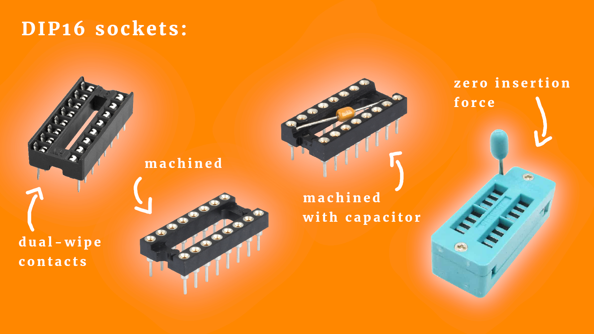
There are identical sockets for all other dual in-line packages as well. The leftmost socket is the simplest version with dual-wipe contacts (a long time ago there used to be single-wipe contacts as well, but those have long been discontinued due to their notorious unreliability). I don't really like to use the dual-wipe sockets because the contact can also be a bit unreliable at times. But hey, they are the cheapest option.
If you want something more reliable, go for a machined socket. I find this is usually a good investment and the contact is far more reliable. You can also find sockets with a built-in 100nF capacitor between pin 8 and 16 (in general: between GND and VDD). This is very useful because it does not use extra space on your breadboard or PCB, but it costs a bit more. I will talk more about this capacitor below.
Last, there is that strange blue-ish object on the right: it is a so-called zero insertion force socket. It is primarily used for testing of CMOS ICs (and any other kind of IC that has a matching socket layout). The idea is that you use the lever on the left to connect the IC electrically with the terminals without applying any force on the IC's pins. With all the other sockets pictured above there is a risk of the fragile pins breaking after about a dozen or so insertions. Needless to say, the zero insertion socket only makes sense for a few ICs in your project, such as memory, controllers, or other expensive integrated circuits.
Okay, but what about that weird 100nF capacitor? In a perfect world we wouldn't need it, but more often than not the power supply rail is a bit noisy, meaning that the supply voltage is not 100% stable. Some CMOS ICs really don't like that, and small capacitors can help smooth out those fluctuations:
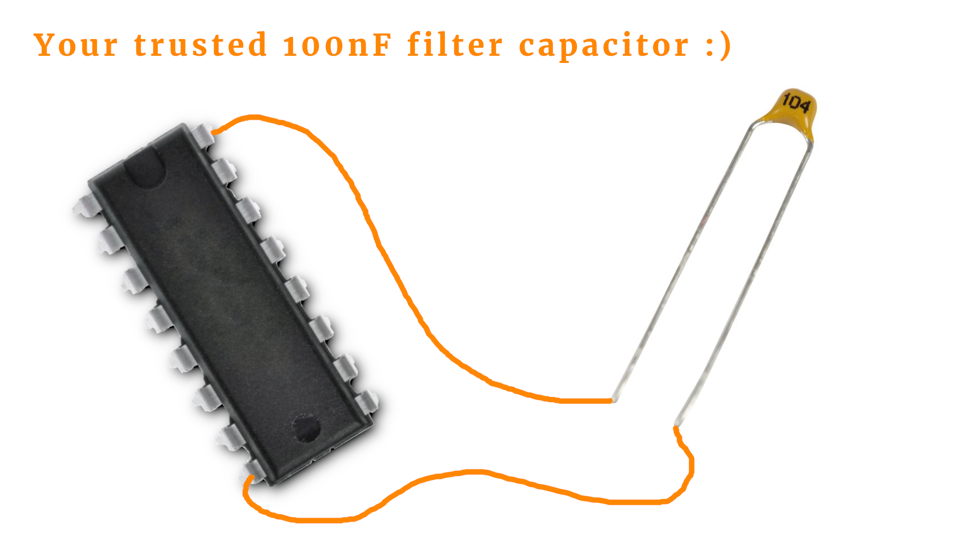
It is a bit more work to put in the 100nF capacitor, but it is worth it because your circuit will be more reliable.
For the rest of this tutorial I will go through some useful CMOS ICs that I have used many many times. It is by no means an exhaustive list, but I find the ones I will mention of particular use :) If I have forgotten to mention your favorite CMOS IC, please get in touch and I will see what I can do!
Decimal counters
Counters are useful devices in electronics. The CD4017 counts from 0-9 (which is why it is called a decimal counter) and you can find the datasheet in the resources box. Here is the pinout:
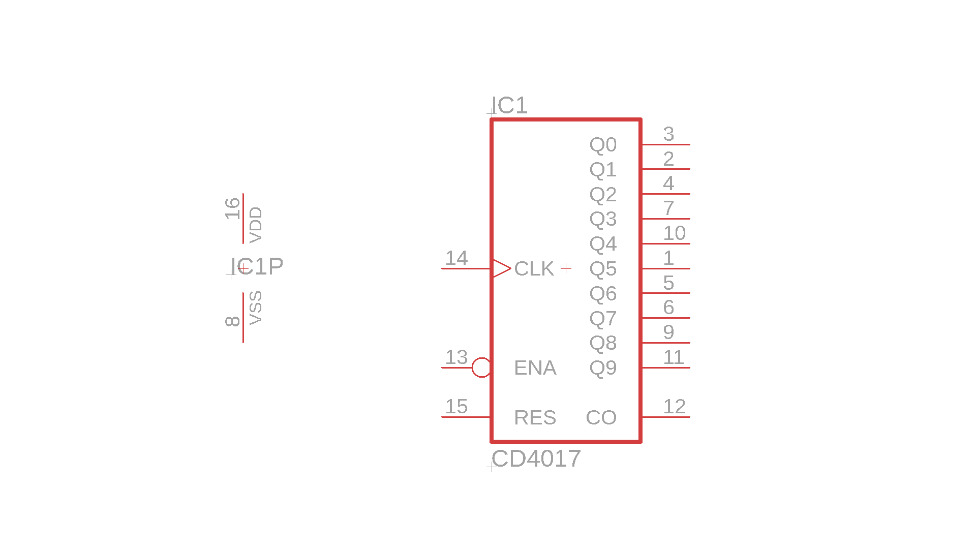
- VDD is the positive terminal and VSS is ground.
- CLK is the clock pin. The counter increases by one on every pulse on this pin.
- Q0-Q9: the current counter value in decimal, meaning that only one of these outputs is on at one time.
- CO is the carry out pin. It has a positive pulse whenever the counter resets from 9 to 0, allowing you to cascade multiple counters.
- RES is the reset pin. When a logical 1 is applied, the counter resets to 0.
- EN stands for enable, but it is an inverted input (as indicated by the little circle). When EN is set to a logical 1, then the counter works as usual. When it is set to a logical 0, then the counter ignores clock pulses and stands still.
The CD4017 is nice if you need ten individual signals to display the current state of the counter. But what if you only need to display it? Then the CD4026 is a better choice (datasheet above):
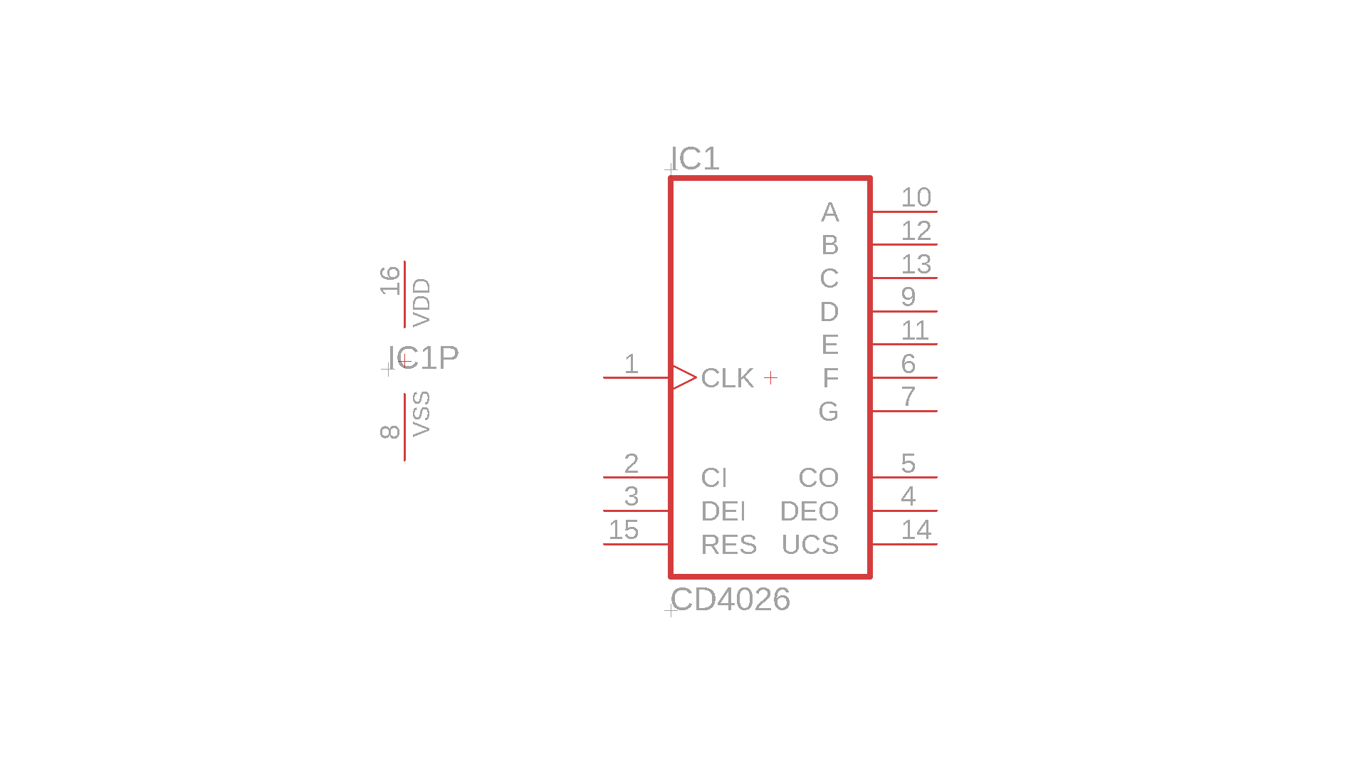
This nifty little IC is a decimal counter t hat directly encodes the counter's value into a 7 segment format.
- VDD is the positive terminal and VSS is ground.
- CLK is the clock pin. The counter increases by one on every pulse on this pin.
- A-G: these pins output the current counter value encoded in seven segments a-g.
- CO is the carry out pin. It has a positive pulse whenever the counter resets from 9 to 0, allowing you to cascade multiple counters.
- RES is the reset pin. When a logical 1 is applied, the counter resets to 0.
- DEI stands for display enable in which means that whenever this pin is held at 1 the display is on, and whenever it is held 0 the display is off. This is the only way to blank the display.
- CI means clock inhibit, and, just as the name suggests, it inhibits the counting function whenever it is set to 1. In other words: if you put CI to a logic high level the counter will ignore pulses on the clock pin. If you want the counter to function normally, CI has to be tied to ground.
- DEO stands for display enable output and just carries the same signal that is applied to DEI.
- UGC is perhaps the most unusual pin, and stands for ungated 'c' segment out. The explanation is very simple, though: because the counter outputs directly in the seven segment format, it is hard to reset it at a precise value. If you look at a 7 segment display, this is how the segments are labeled:
As you track through the numbers, starting at 1, the 'c' segment turns OFF the first time at the number 2. Therefore this segment can be used to find out when the counter arrives at 2 for the first time.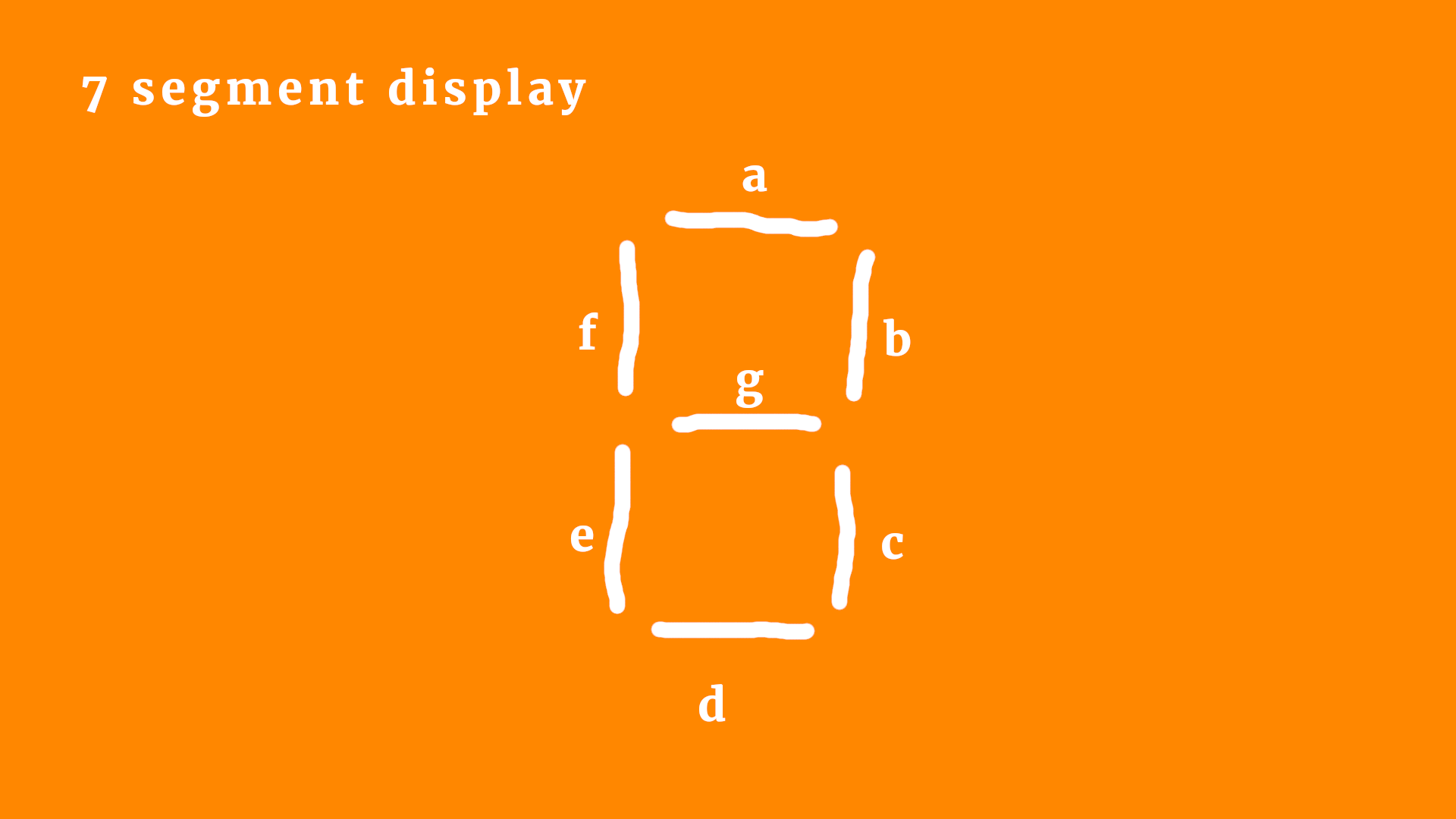
The CD4026 is a bit of an oddball that way, but it sure is a neat little IC when you need a one or more digit counter. Resetting it, however, can prove a bit difficult (but it is of course always possible).
Binary counters
Okay, counting in decimal is nice for the human eye, but it is not very efficient because we require a lot of pins for very limited information. This is why sometimes binary counters are useful. Here is the CD4020, which is a 14-bit counter (datasheet above). If you are wondering, it counts from 0 to 16383, which is quite a lot:
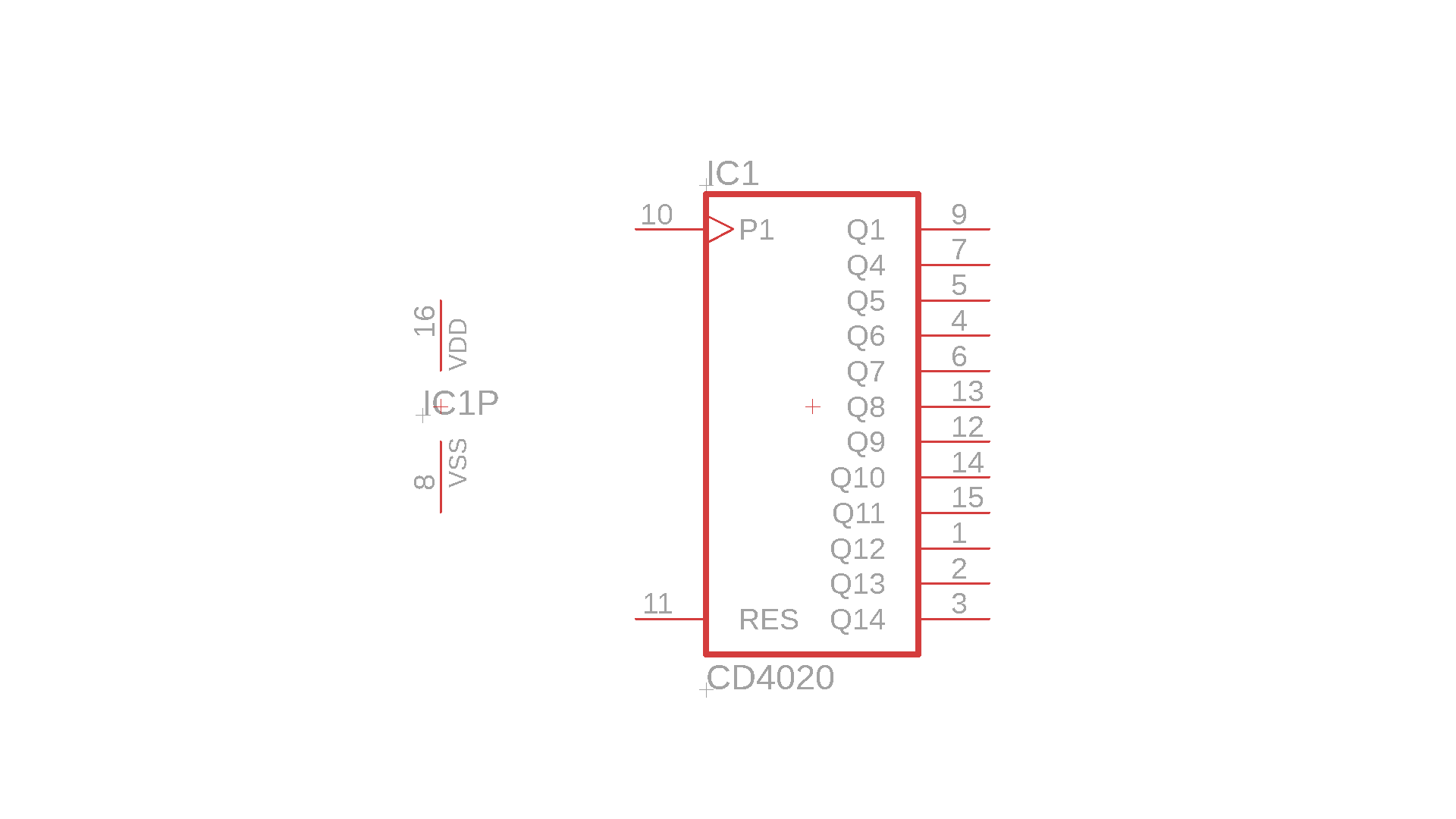
- VDD is the positive terminal and VSS is ground.
- P1 serves as the clock pin. The counter increases by one on every pulse on this pin.
- The pins Q1 as well as Q4-14 output the counter's value in binary. Where are pins Q2 and Q3? They don't exist! This may sound a bit silly, but it actually makes sense in a lot of applications when you don't need a lot of resolution. Moreover, this way the counter fits into a standard DIP16 package (otherwise the package would have to be DIP18 due to the two more additional pins).
But rest assured, you can also find full counters that don't skip any outputs. Here is an example, the CD4024 (datasheet above):
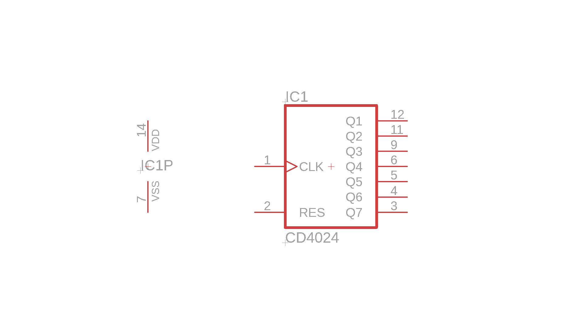
Everything works exactly as with the CD4020, only now there are all outputs from Q1-Q7 (counting from 0 to 127), and the CLK serves as the clock pin.
BCD counter
I tend to think of the CD4510 as a binary-coded decimal counter (BCD counter), but that is strictly speaking not correct. The CD4510 is a 4-bit binary counter, counting from 0 to 15 (datasheet above). It can also be preset to a certain value, and you can control the direction of counting as well. It is a very common choice for clock circuits, and in that case I often used it in conjunction with the CD4511 (see below) as a BCD counter. At any rate, here is the CD4510:
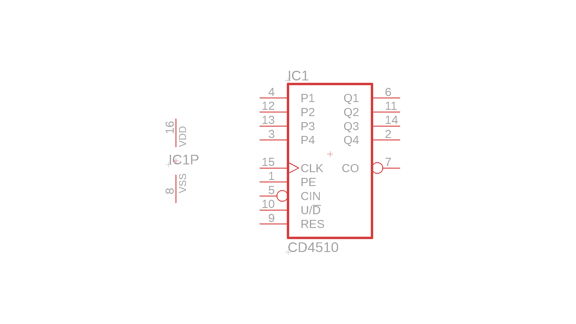
- VDD is the positive terminal and VSS is ground.
- CLK is the clock pin. The counter increases by one on every pulse on this pin.
- Q1-Q4: these pins output the current counter value in binary.
- CO is the inverted carry out pin. It has a negative pulse (meaning it goes from 1 to 0 back to 1) whenever the counter resets from 15 to 0, allowing you to cascade multiple counters.
- RES is the reset pin. When a logical 1 is applied, the counter resets to 0.
- CI means carry in. It can be used to cascade multiple counters by connecting it to the carry out pin of a less significant counter stage. In this setup, the clock pins of all stages need to be connected in parallel.
- P1-P4 are the preset pins. Here you can set the value in binary that the counter is supposed to take as a preset value.
- PE stands for preset enable, and whenever this pin is high, the current state of the pints P1-P4 will be applied to Q1-Q4. This way you can instantaneously set the counter to any value between 0 and 15.
- U/D is where you tell the CD4510 whether it counts up or down. When U/D is set to high, the CD4510 counts up, and when it is set to low, it counts down.
This device is a bit involved, but it is quite versatile if you need a bit more functionality.
Logic gates
Now for something entirely different: logic gates! These are devices that combine several input signals to one output signal, and you can find all datasheets above. I won't go into a lot of detail here (maybe in a future article) but I hope you get the main idea. There are dozens of different CMOS ICs out there, which is why I only collected a few examples in this article. Here we go:
The CD4094 contains six inverters:
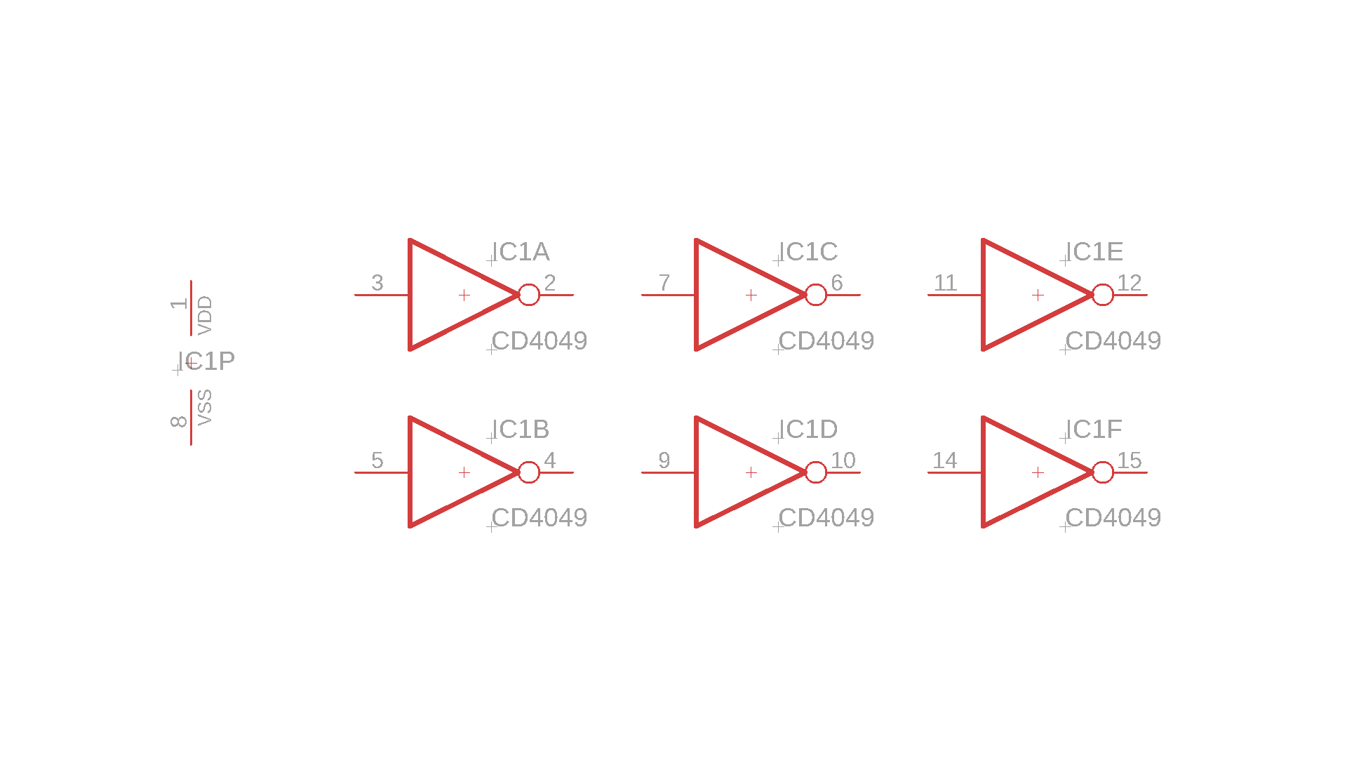
All these six devices are included in the package of one CD4049 chip, which is quite convenient. Each one of these simply inverts the signal at the input. Let's look at the first inverter, here called IC1A. If pin 3 is high then pin 2 is low, and if pin 3 is low then pin 2 is high. You get the idea :)
The CD4081 has four AND gates:
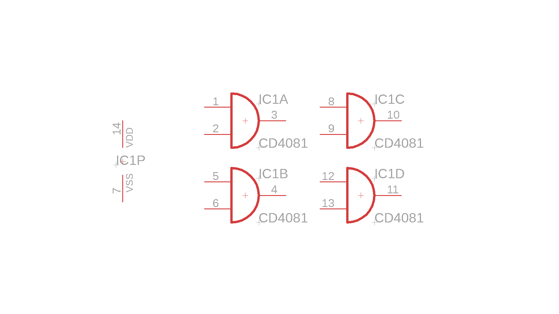
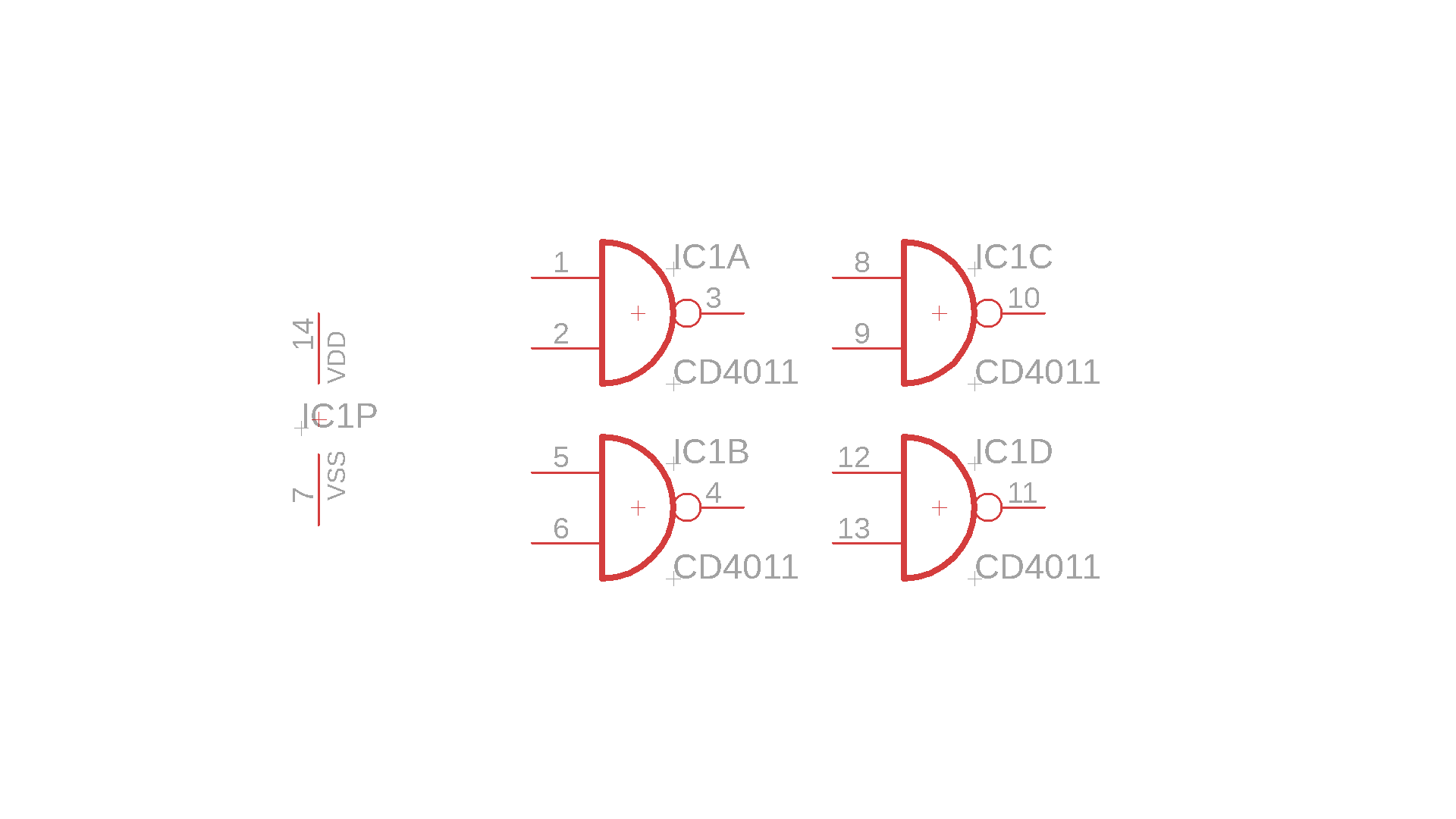
Let's look at IC1A again. Only of both pins 1 AND 2 are high then pin 3 is high, otherwise it is low.
The CD4071 has four OR gates:

If pin 1, pin 2, or pin 1 and pin 2 are high, then pin 3 is high, otherwise it is low. The CD4070, on the other hand, has four exclusive OR gates, also called XOR gates:

If pin 1 is high, or pin 2 is high, then pin 3 is high. But if both pin 1 AND pin 2 are high, then pin 3 is low. This is different from the OR gate! It is easy to remember: the output of these XOR gates is high whenever the two inouts are different.
The following CD 4001 is another interesting concoction: it is a so-called NOR gate. It is an OR gate where the output is inverted:
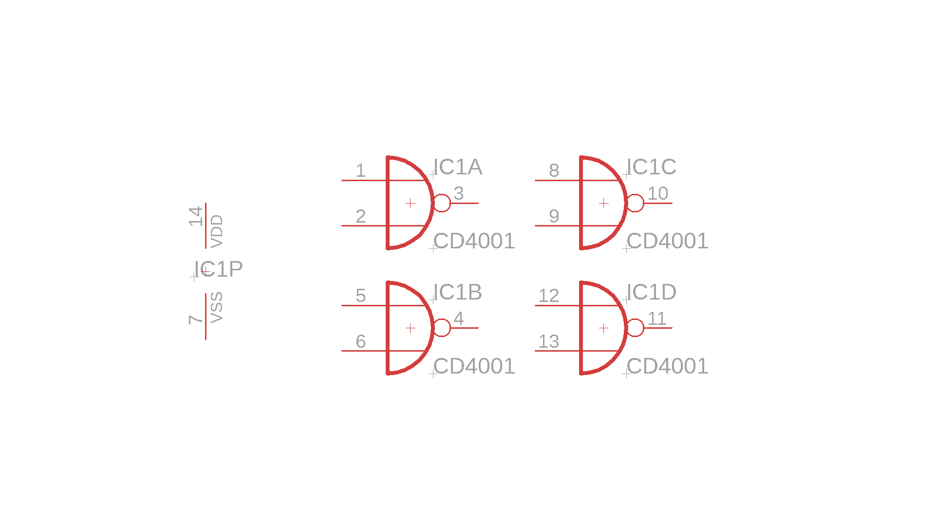
Similarly the CD4011 corresponds to a so-called NAND gate, which is an inverted AND gate:
Maybe this was confusing, but logic gates are very simple objects that can be very helpful sometimes. Say we want to reset the CD4026 7-segment counter at number 3. At a displayed number 3, see the diagram above, the segments a,b,c,d, and g are ON whereas the segments e and f are OFF. Using logic gates we could check for this condition and connect the output to the reset input of the CD4026 :)
Decoders
Decoders are usually employed when a counter's signal needs to be converted into a human-readable format. The CD4028 turns a binary-coded decimal (BCD) value from 0...9 into a decimal output:
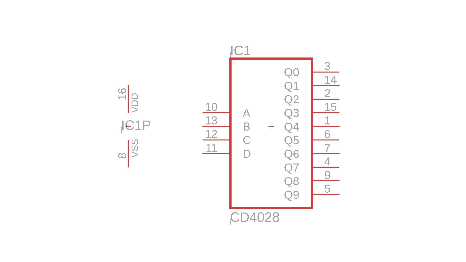
- VDD is the positive terminal and VSS is ground.
- A-D are bits 0 to 3 of the BCD signal.
- Q0-Q9 are the ten decimal outputs.
The CD4511, on the other hand, takes a BCD signal and converts it into 7 segment format:
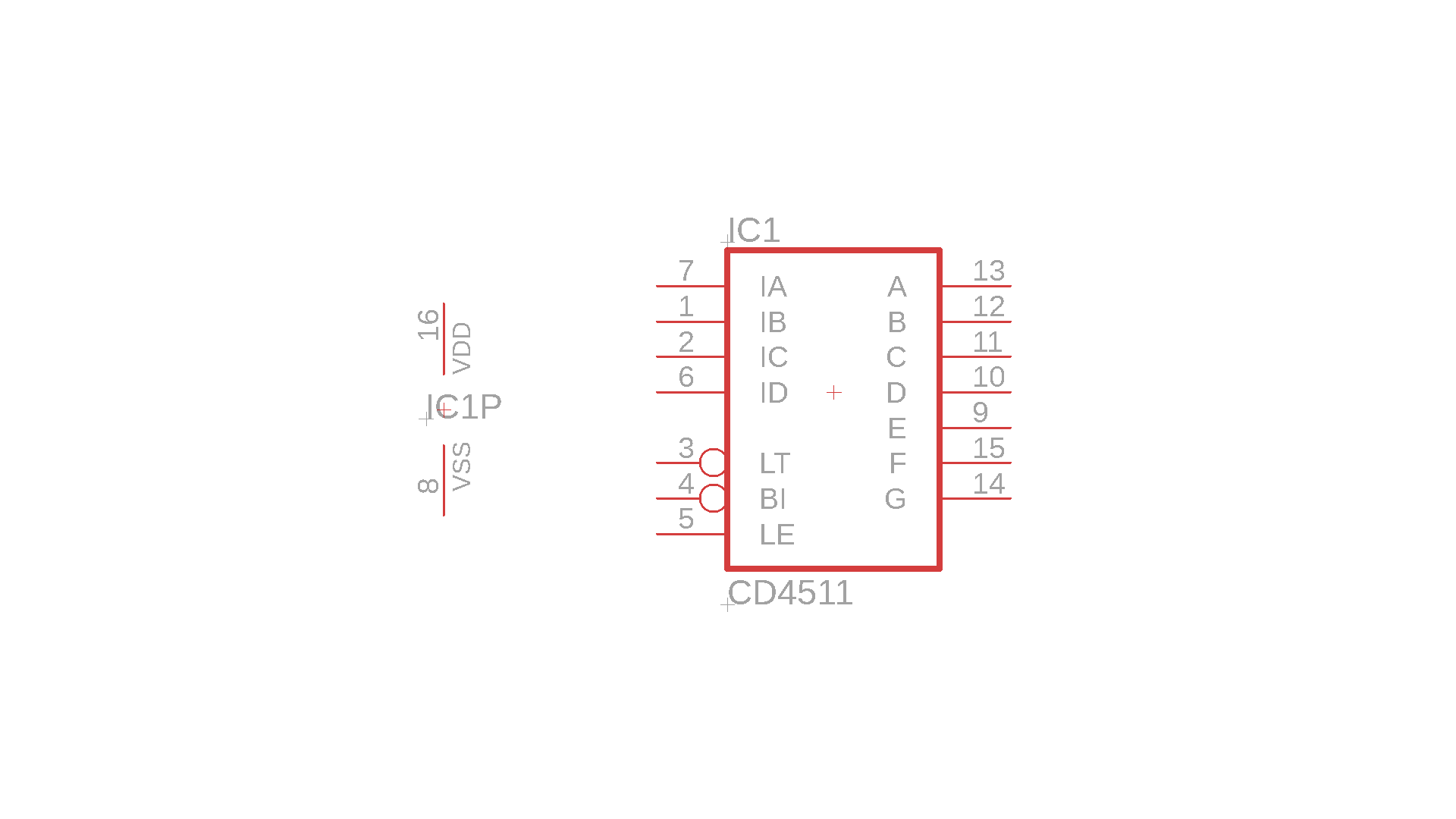
- VDD is the positive terminal and VSS is ground.
- IA-ID are bits 0 to 3 of the BCD signal.
- A-G are the 7 segment outputs.
- LT stands for lamp test and is an inverted input. If it is set to low, then all segments are turned ON. This is useful to check if all segments work correctly. During normal operation this pin needs to be set high.
- BI means blanking (I don't know why it says BI and not just B) and is also an inverted input. Setting it low blanks the display, and setting it high guarantees normal operation. It is in some sense the opposite of the LT pin. It can also be used in combination with a PWM signal to modulate the display's brightness.
- LE stands for latch enable. Its function is very similar to that of the STROBE pin on the CD4094 shift register": whenever it is set to 0, the value on pines IA-ID is encoded into 7 segment, but when it is set to high then the input on IA-ID is ignored. This way one can use the same IA-ID-lines for multiple CD4511 chips :)
Shift register
For completeness I also want to mention the shift register CD4094 that we talked about last week:
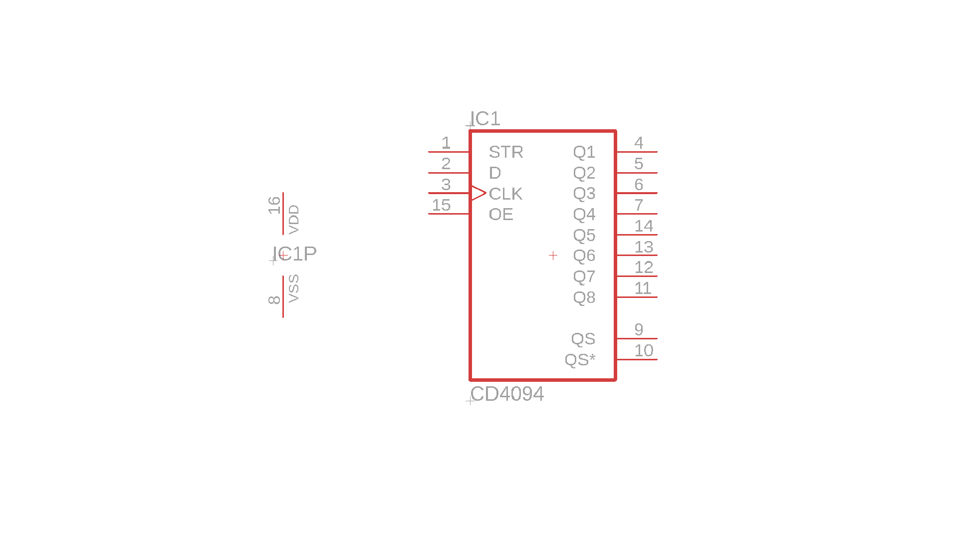
You can find the datasheet here. This is a device that can serve as an interface between a microcontroller and associated CMOS logic chips. I won't explain all the details here since we already learned about it last week.
...and so much more!

I hope I could give you a glimpse into the fascinating world of CMOS technology. There are so many integrated circuits out there, and it does not hurt to know that they exist, even if you work with microcontrollers. We omitted quite a bunch of other devices, including multiplexers, flip flops, adders, and much more. I still hope that this article has sparked your interest. Thanks for reading!